Silicon
Carbon Compounds, Inorganic
Silicon Dioxide
Nanowires
Semiconductors
Nanotechnology
Porosity
Transistors, Electronic
Silicic Acid
Germanium
Electronics
Silanes
Surface Properties
Biosensing Techniques
Nanostructures
Micro-Electrical-Mechanical Systems
Microtechnology
Silicones
Hafnium
Diatoms
Equipment Failure Analysis
Microscopy, Electron, Scanning
Nanopores
Lab-On-A-Chip Devices
Optical Devices
A new principle for rapid immunoassay of proteins based on in situ precipitate-enhanced ellipsometry. (1/770)
A new technique is presented that allows measurement of protein concentrations in the picomolar range with an assay time of only 10-20 min. The method is an enzyme-linked immunosorbent assay (ELISA), but uses in-situ ellipsometric measurement of a precipitating enzyme product instead of the usual colorimetric detection of accumulating enzyme product in solution. Quantitative validation was obtained by use of annexin V, a protein with high binding affinity for phosphatidylserine-containing phospholipid membranes, resulting in a transport-limited adsorption rate. This property was exploited to obtain a range of low surface concentrations of annexin V by timed exposures of phospholipid bilayers to known concentrations of annexin V. Using polyvinylchloride (PVC)-coated and silanized silicon slides, various versions of this technique were used for the rapid assay of fatty acid-binding protein (FABP), a recently introduced early marker for acute myocardial infarction with a normal plasma concentration below 1 nmol/l, interleukin 6 (IL-6), a cytokine with normal plasma concentrations below 1 pmol/l, and again, annexin V. A possible future application of the method in the development of a one-step ELISA is discussed. (+info)Crystalline silica exposure, radiological silicosis, and lung cancer mortality in diatomaceous earth industry workers. (2/770)
BACKGROUND: The role of silicosis as either a necessary or incidental condition in silica associated lung cancer remains unresolved. To address this issue a cohort analysis of dose-response relations for crystalline silica and lung cancer mortality was conducted among diatomaceous earth workers classified according to the presence or absence of radiological silicosis. METHODS: Radiological silicosis was determined by median 1980 International Labour Organisation system readings of a panel of three "B" readers for 1809 of 2342 white male workers in a diatomaceous earth facility in California. Standardised mortality ratios (SMR) for lung cancer, based on United States rates for 1942-94, were calculated separately for workers with and without radiological silicosis according to cumulative exposures to respirable crystalline silica (milligrams per cubic meter x years; mg/m3-years) lagged 15 years. RESULTS: Eighty one cases of silicosis were identified, including 77 with small opacities of > or = 1/0 and four with large opacities. A slightly larger excess of lung cancer was found among the subjects with silicosis (SMR 1.57, 95% confidence interval (CI) 0.43 to 4.03) than in workers without silicosis (SMR 1.19, 95% CI 0.87 to 1.57). An association between silica exposure and lung cancer risk was detected among those without silicosis; a statistically significant (p = 0.02) increasing trend of lung cancer risk was seen with cumulative exposure, with SMR reaching 2.40 (95% CI 1.24 to 4.20) at the highest exposure level (> or = 5.0 mg/m3-years). A similar statistically significant (p = 0.02) dose-response gradient was observed among non-silicotic subjects when follow up was truncated at 15 years after the final negative radiograph (SMR 2.96, 95% CI 1.19 to 6.08 at > or = 5.0 mg/m3-years), indicating that the association among non-silicotic subjects was unlikely to be accounted for by undetected radiological silicosis. CONCLUSIONS: The dose-response relation observed between cumulative exposure to respirable crystalline silica and lung cancer mortality among workers without radiological silicosis suggests that silicosis is not a necessary co-condition for silica related lung carcinogenesis. However, the relatively small number of silicosis cases in the cohort and the absence of radiographic data after employment limit interpretations. (+info)Chip-based genotyping by mass spectrometry. (3/770)
Silicon chips with immobilized target DNAs were used for accurate genotyping by mass spectrometry. Genomic DNAs were amplified with PCR, and the amplified products were covalently attached to chip wells via N-succinimidyl (4-iodoacetyl)aminobenzoate (SIAB) chemistry. Primer annealing, extension, and termination were performed on a 1-microl scale directly in the chip wells in parallel. Diagnostic products thus generated were detected in situ by using matrix-assisted laser desorption ionization mass spectrometry. This miniaturized method has the potential for accurate, high-throughput, low-cost identification of genetic variations. (+info)Thin film biosensor for rapid visual detection of nucleic acid targets. (4/770)
BACKGROUND: We have developed a silicon-based biosensor that generates a visual signal in response to nucleic acid targets. METHODS: In this system, capture oligonucleotide probes are immobilized on the surface of the biosensor. Interaction of the capture probes with a complementary target and a biotinylated detector oligonucleotide allows initiation of formation of an organic thin film on the biosensor. Thin film formation is completed by enzymatic activity of peroxidase conjugated to an anti-biotin antibody. Peroxidase catalyzes deposition of an insoluble product onto the silicon surface, generating a uniform thin film. The increased thickness on the surface alters the perceived color of the biosensor through changes in the interference patterns of reflected light from the surface, causing a color change from gold to purple. RESULTS: The biosensor results may be evaluated by direct visual inspection or quantified by ellipsometry. Results are obtained in 25 min with a detection limit of 5 pmol/L (150 amol/sample). Selectivity of the biosensor is demonstrated by discrimination of single nucleotide mismatches. Multitarget arrays are also analyzed with the thin film biosensor, and the system is capable of detecting targets from human serum and urine. CONCLUSIONS: The biosensor surface is inexpensive to produce, and the assay format is simple and rapid. The thin film biosensor is adaptable to a wide variety of nucleic acid detection applications, including rapid diagnostic testing for infectious disease panels, antibiotic resistance panels, or allelic discrimination of specific genetic markers. (+info)Stable five- and six-coordinated silicate anions in aqueous solution. (5/770)
Addition of aliphatic polyols to aqueous silicate solutions is shown to yield high concentrations of stable polyolate complexes containing five- or six-coordinated silicon. Coordinating polyols require at least four hydroxy groups, two of which must be in threo configuration, and coordinate to silicon via hydroxy oxygens at chain positions on either side of the threo pair. The remarkable ease by which these simple sugar-like molecules react to form hypervalent silicon complexes in aqueous solution supports a long-standing supposition that such species play a significant role in the biological uptake and transport of silicon and in mineral diagenesis. (+info)Patterned deposition of cells and proteins onto surfaces by using three-dimensional microfluidic systems. (6/770)
Three-dimensional microfluidic systems were fabricated and used to pattern proteins and mammalian cells on a planar substrate. The three-dimensional topology of the microfluidic network in the stamp makes this technique a versatile one with which to pattern multiple types of proteins and cells in complex, discontinuous structures on a surface. The channel structure, formed by the stamp when it is in contact with the surface of the substrate, limits migration and growth of cells in the channels. With the channel structure in contact with the surface, the cells stop dividing once they form a confluent layer. Removal of the stamp permits the cells to spread and divide. (+info)In situ self hardening bioactive composite for bone and dental surgery. (7/770)
A new biomaterial is presented which consists of a cellulose derivative--silanised hydroxyethylcellulose (HEC-SIL) and biphasic calcium phosphate (BCP). Rheological properties of the polymer itself and its mixture with BCP are pH-dependent. At pH 10-12 HEC-SIL is liquid and undergoes quick gellation at pH < 9. Similarly, the paste of HEC-SIL and BCP is fluid and injectable at higher pH and solidifies in biological solutions. The rate of this solidification can be easily controlled by the degree of substitution of hydroxyethylcellulose with silicoalkoxy groups. (+info)Oligomeric but not monomeric silica prevents aluminum absorption in humans. (8/770)
BACKGROUND: Soluble silica, a ubiquitous component of the diet, may be the natural ligand for dietary aluminum and may prevent its accumulation and toxicity in animals. However, previous studies on the inhibition of aluminum absorption and toxicity by soluble silica have produced conflicting results. We recently identified a soluble silica polymer, oligomeric silica, that has a much higher affinity for aluminum than does monomeric silica and that may be involved in the sequestration of aluminum. OBJECTIVE: By using (26)Al as a tracer, we investigated the effects of oligomeric and monomeric silica on the bioavailability of aluminum (study 1) and compared the availability of silicon from oligomeric and monomeric silica in the human gastrointestinal tract (study 2). DESIGN: In study 1, three healthy volunteers each ingested aluminum alone (control), aluminum with oligomeric silica (17 mg), and aluminum with monomeric silica (17 mg). In study 2, five healthy volunteers ingested both the oligomeric and monomeric forms of silica (34 mg). Serum and urine samples were analyzed for aluminum and silicon. RESULTS: Oligomeric silica reduced the availability of aluminum by 67% (P = 0.01) compared with the control, whereas monomeric silica had no effect (P = 0.40). Monomeric silica was readily taken up from the gastrointestinal tract and then excreted in urine (53%), whereas oligomeric silica was not detectably absorbed or excreted. CONCLUSIONS: The oligomeric, high-aluminum-affinity form of soluble silica reduces aluminum availability from the human gastrointestinal tract. Its potential role in the amelioration of aluminum toxicity in other biological systems requires attention. (+info)I'm sorry for any confusion, but "Silicon" does not have a specific medical definition. Silicon is a chemical element with the symbol Si and atomic number 14. It is a metalloid, which means it has properties of both metals and nonmetals. In the human body, silicon is not considered an essential nutrient, although it is found in trace amounts in various tissues. Some research suggests that silicon might play a role in collagen synthesis and bone health, but more studies are needed to confirm these findings and establish recommended intake levels.
Silicon compounds refer to chemical substances that contain the element silicon (Si) combined with other elements. Silicon is a Group 14 semimetal in the periodic table, and it often forms compounds through covalent bonding. The most common silicon compound is silicon dioxide (SiO2), also known as silica, which is found in nature as quartz, sand, and other minerals.
Silicon can form compounds with many other elements, including hydrogen, oxygen, halogens, sulfur, nitrogen, and carbon. For example:
* Silanes (SiHn) are a series of silicon-hydrogen compounds where n ranges from 1 to 6.
* Silicones are synthetic polymers made up of alternating silicon and oxygen atoms with organic groups attached to the silicon atoms.
* Silicates are a class of minerals that contain silicon, oxygen, and one or more metal cations. They have a wide range of structures and uses, including as building materials, ceramics, and glass.
* Siloxanes are a group of compounds containing alternating silicon-oxygen bonds with organic groups attached to the silicon atoms.
Silicon compounds have various applications in industry, medicine, and daily life. For instance, silicones are used in medical devices such as breast implants, contact lenses, and catheters due to their biocompatibility and flexibility. Silicates are found in pharmaceuticals, cosmetics, and food additives. Silicon-based materials are also used in dental restorations, bone cement, and drug delivery systems.
Carbon inorganic compounds are chemical substances that contain carbon combined with one or more elements other than hydrogen. These compounds include oxides of carbon such as carbon monoxide (CO) and carbon dioxide (CO2), metal carbides like calcium carbide (CaC2) and silicon carbide (SiC), and carbonates like calcium carbonate (CaCO3) and sodium carbonate (Na2CO3).
Unlike organic compounds, which are based on carbon-hydrogen bonds, inorganic carbon compounds do not contain hydrocarbon structures. Instead, they feature carbon bonded to elements such as nitrogen, oxygen, sulfur, or halogens. Inorganic carbon compounds have diverse physical and chemical properties and play important roles in various industrial applications, as well as in biological systems.
Silicon dioxide is not a medical term, but a chemical compound with the formula SiO2. It's commonly known as quartz or sand and is not something that would typically have a medical definition. However, in some cases, silicon dioxide can be used in pharmaceutical preparations as an excipient (an inactive substance that serves as a vehicle or medium for a drug) or as a food additive, often as an anti-caking agent.
In these contexts, it's important to note that silicon dioxide is considered generally recognized as safe (GRAS) by the U.S. Food and Drug Administration (FDA). However, exposure to very high levels of respirable silica dust, such as in certain industrial settings, can increase the risk of lung disease, including silicosis.
I'm sorry for any confusion, but "nanowires" is not a medical term. It is a term used in the field of materials science and nanotechnology. Nanowires are one-dimensional structures with a diameter of 1-100 nanometers (nm) and an aspect ratio (length/diameter) greater than 1000. They have unique electrical, mechanical, and optical properties that make them useful in various applications such as electronics, sensors, energy storage, and biomedical devices.
I'm sorry for any confusion, but "semiconductors" is a term from the field of materials science and electronics rather than medicine. Semiconductors are materials, often silicon-based, that have properties between conductors and insulators. They are used in various electronic devices due to their unique property of controlling the flow of electrical current. If you have any medical questions, I'd be happy to help with those instead!
Organosilicon compounds are a class of chemical compounds that contain at least one organic group (a group of atoms composed mainly of carbon and hydrogen) bonded to a silicon atom. The organic group can be an alkyl group, aryl group, or any other group that is derived from a hydrocarbon.
The term "organosilicon" is used to describe the covalent bond between carbon and silicon atoms, which is a type of bond known as a "sigma bond." This bond is formed by the overlap of atomic orbitals between the carbon and silicon atoms. The resulting organosilicon compound can have a wide range of physical and chemical properties, depending on the nature of the organic group and the number of such groups attached to the silicon atom.
Organosilicon compounds are widely used in various industries, including electronics, coatings, adhesives, and pharmaceuticals. They are also used as intermediates in the synthesis of other chemical compounds. Some common examples of organosilicon compounds include silicones, which are polymers that contain repeating units of siloxane (Si-O-Si) bonds, and organofunctional silanes, which are used as coupling agents to improve the adhesion of materials to surfaces.
Nanotechnology is not a medical term per se, but it is a field of study with potential applications in medicine. According to the National Nanotechnology Initiative, nanotechnology is defined as "the understanding and control of matter at the nanoscale, at dimensions between approximately 1 and 100 nanometers, where unique phenomena enable novel applications."
In the context of medicine, nanotechnology has the potential to revolutionize the way we diagnose, treat, and prevent diseases. Nanomedicine involves the use of nanoscale materials, devices, or systems for medical applications. These can include drug delivery systems that target specific cells or tissues, diagnostic tools that detect biomarkers at the molecular level, and tissue engineering strategies that promote regeneration and repair.
While nanotechnology holds great promise for medicine, it is still a relatively new field with many challenges to overcome, including issues related to safety, regulation, and scalability.
In the context of medical terminology, "porosity" is not a term that is frequently used to describe human tissues or organs. However, in dermatology and cosmetics, porosity refers to the ability of the skin to absorb and retain moisture or topical treatments.
A skin with high porosity has larger pores and can absorb more products, while a skin with low porosity has smaller pores and may have difficulty absorbing products. It is important to note that this definition of porosity is not a medical one but is instead used in the beauty industry.
I'm sorry for any confusion, but "Transistors, Electronic" is not a recognized medical term. Transistors are electronic components used in various devices, including medical equipment, to amplify or switch electronic signals and electrical power. They are crucial for the functioning of numerous technologies, such as computers, smartphones, and other digital devices. However, they are not typically described in the context of medical definitions. If you have any questions related to electronics or technology that you believe could be relevant to a medical context, please provide more details so I can give a more accurate response.
I'm sorry for any confusion, but "Silicic Acid" is not a recognized medical term. Silicic acid, also known as orthosilicic acid, is a compound that contains silicon and oxygen in a ratio of 1:2 (Si(OH)4). It's commonly found in water, soil, and various plants.
In the context of health and medicine, silica or silicic acid supplements are sometimes used for their potential benefits to bone health, collagen production, and hair and nail growth. However, more research is needed to fully understand these effects and their optimal usage.
If you have any questions related to a specific medical condition or treatment, I would recommend consulting with a healthcare professional.
I'm sorry for any confusion, but "Germanium" is not a medical term. It is a chemical element with the symbol Ge and atomic number 32. Germanium is a lustrous, hard, grayish-white metalloid in the carbon group, chemically similar to its neighbor silicon.
It's primarily used in the electronics industry for semiconductors and fiber optic systems due to its properties as a semiconductor. If you have any questions related to medical terminology or concepts, I'd be happy to help with those!
I believe there might be a misunderstanding in your question. "Electronics" is not a medical term, but rather a branch of physics and engineering that deals with the design, construction, and operation of electronic devices and systems. It involves the study and application of electrical properties of materials, components, and systems, and how they can be used to process, transmit, and store information and energy.
However, electronics have numerous applications in the medical field, such as in diagnostic equipment, monitoring devices, surgical tools, and prosthetics. In these contexts, "electronics" refers to the specific electronic components or systems that are used for medical purposes.
Silanes are a group of chemical compounds that contain silicon and hydrogen. The general formula for silanes is Si_xH_(2x+2), where x is a positive integer. Silanes are named after their parent compound, silane (SiH4), which contains one silicon atom and four hydrogen atoms.
Silanes are colorless and highly flammable gases at room temperature. They are typically prepared by the reaction of metal silicides with acids or by the reduction of halogenated silanes. Silanes have a variety of industrial applications, including as intermediates in the production of silicon-based materials such as semiconductors and polymers.
In medical contexts, silanes are not typically used directly. However, some silane-containing compounds have been investigated for their potential therapeutic uses. For example, some organosilanes have been shown to have antimicrobial properties and may be useful as disinfectants or in the development of medical devices. Other silane-containing materials have been studied for their potential use in drug delivery systems or as imaging agents in diagnostic procedures.
It is important to note that some silanes can be hazardous if not handled properly, and they should only be used by trained professionals in a controlled environment. Exposure to silanes can cause irritation to the eyes, skin, and respiratory tract, and prolonged exposure can lead to more serious health effects.
I'm sorry for any confusion, but "Solar Energy" is not a term typically used in medical definitions. Solar energy refers to the energy that comes from the sun and can be captured and converted into thermal or electrical energy. It is not a medical concept or treatment. If you have any questions related to health or medicine, I'd be happy to try to help answer those for you!
Surface properties in the context of medical science refer to the characteristics and features of the outermost layer or surface of a biological material or structure, such as cells, tissues, organs, or medical devices. These properties can include physical attributes like roughness, smoothness, hydrophobicity or hydrophilicity, and electrical conductivity, as well as chemical properties like charge, reactivity, and composition.
In the field of biomaterials science, understanding surface properties is crucial for designing medical implants, devices, and drug delivery systems that can interact safely and effectively with biological tissues and fluids. Surface modifications, such as coatings or chemical treatments, can be used to alter surface properties and enhance biocompatibility, improve lubricity, reduce fouling, or promote specific cellular responses like adhesion, proliferation, or differentiation.
Similarly, in the field of cell biology, understanding surface properties is essential for studying cell-cell interactions, cell signaling, and cell behavior. Cells can sense and respond to changes in their environment, including variations in surface properties, which can influence cell shape, motility, and function. Therefore, characterizing and manipulating surface properties can provide valuable insights into the mechanisms of cellular processes and offer new strategies for developing therapies and treatments for various diseases.
Biosensing techniques refer to the methods and technologies used to detect and measure biological molecules or processes, typically through the use of a physical device or sensor. These techniques often involve the conversion of a biological response into an electrical signal that can be measured and analyzed. Examples of biosensing techniques include electrochemical biosensors, optical biosensors, and piezoelectric biosensors.
Electrochemical biosensors measure the electrical current or potential generated by a biochemical reaction at an electrode surface. This type of biosensor typically consists of a biological recognition element, such as an enzyme or antibody, that is immobilized on the electrode surface and interacts with the target analyte to produce an electrical signal.
Optical biosensors measure changes in light intensity or wavelength that occur when a biochemical reaction takes place. This type of biosensor can be based on various optical principles, such as absorbance, fluorescence, or surface plasmon resonance (SPR).
Piezoelectric biosensors measure changes in mass or frequency that occur when a biomolecule binds to the surface of a piezoelectric crystal. This type of biosensor is based on the principle that piezoelectric materials generate an electrical charge when subjected to mechanical stress, and this charge can be used to detect changes in mass or frequency that are proportional to the amount of biomolecule bound to the surface.
Biosensing techniques have a wide range of applications in fields such as medicine, environmental monitoring, food safety, and biodefense. They can be used to detect and measure a variety of biological molecules, including proteins, nucleic acids, hormones, and small molecules, as well as to monitor biological processes such as cell growth or metabolism.
Nanostructures, in the context of medical and biomedical research, refer to materials or devices with structural features that have at least one dimension ranging between 1-100 nanometers (nm). At this size scale, the properties of these structures can differ significantly from bulk materials, exhibiting unique phenomena that are often influenced by quantum effects.
Nanostructures have attracted considerable interest in biomedicine due to their potential applications in various areas such as drug delivery, diagnostics, regenerative medicine, and tissue engineering. They can be fabricated from a wide range of materials including metals, polymers, ceramics, and carbon-based materials.
Some examples of nanostructures used in biomedicine include:
1. Nanoparticles: These are tiny particles with at least one dimension in the nanoscale range. They can be made from various materials like metals, polymers, or lipids and have applications in drug delivery, imaging, and diagnostics.
2. Quantum dots: These are semiconductor nanocrystals that exhibit unique optical properties due to quantum confinement effects. They are used as fluorescent labels for bioimaging and biosensing applications.
3. Carbon nanotubes: These are hollow, cylindrical structures made of carbon atoms arranged in a hexagonal lattice. They have exceptional mechanical strength, electrical conductivity, and thermal stability, making them suitable for various biomedical applications such as drug delivery, tissue engineering, and biosensors.
4. Nanofibers: These are elongated nanostructures with high aspect ratios (length much greater than width). They can be fabricated from various materials like polymers, ceramics, or composites and have applications in tissue engineering, wound healing, and drug delivery.
5. Dendrimers: These are highly branched, nanoscale polymers with a well-defined structure and narrow size distribution. They can be used as drug carriers, gene delivery vehicles, and diagnostic agents.
6. Nanoshells: These are hollow, spherical nanoparticles consisting of a dielectric core covered by a thin metallic shell. They exhibit unique optical properties that make them suitable for applications such as photothermal therapy, biosensing, and imaging.
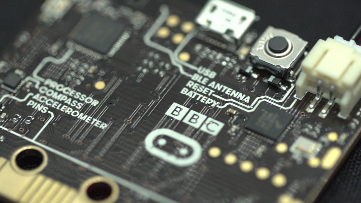
Micro-Electrical-Mechanical Systems (MEMS) is not a medical term, but rather a technology term that refers to the integration of mechanical elements, sensors, actuators, and electronic components on a single silicon chip through microfabrication technology. MEMS devices are extremely small (typically measured in micrometers or millionths of a meter), and can be found in various consumer products such as accelerometers in smartphones and automobiles, inkjet printheads, and biosensors.
In the medical field, MEMS technology has been used to develop various diagnostic and therapeutic devices, including lab-on-a-chip platforms for point-of-care diagnostics, drug delivery systems, and implantable sensors for monitoring physiological parameters such as glucose levels or blood pressure.
Therefore, while MEMS is not a medical definition itself, it is a technology that has significant applications in the medical field.
Equipment design, in the medical context, refers to the process of creating and developing medical equipment and devices, such as surgical instruments, diagnostic machines, or assistive technologies. This process involves several stages, including:
1. Identifying user needs and requirements
2. Concept development and brainstorming
3. Prototyping and testing
4. Design for manufacturing and assembly
5. Safety and regulatory compliance
6. Verification and validation
7. Training and support
The goal of equipment design is to create safe, effective, and efficient medical devices that meet the needs of healthcare providers and patients while complying with relevant regulations and standards. The design process typically involves a multidisciplinary team of engineers, clinicians, designers, and researchers who work together to develop innovative solutions that improve patient care and outcomes.
I'm sorry for any confusion, but "Microtechnology" is not a term that has a specific medical definition. Microtechnology generally refers to the development and application of technologies on a microscopic or tiny scale. It is used in various fields including engineering, physics, electronics, and materials science.
In the context of medicine, microtechnologies can be used in the development of medical devices, diagnostic tools, drug delivery systems, and other healthcare applications. For example, microfabrication techniques are used to create microfluidic devices for lab-on-a-chip applications, which can perform complex biochemical analyses for disease diagnosis or drug screening.
However, it's important to note that the application of microtechnologies in medicine is constantly evolving, and new developments and techniques are being explored all the time.
Silicones are not a medical term, but they are commonly used in the medical field, particularly in medical devices and healthcare products. Silicones are synthetic polymers made up of repeating units of siloxane, which is a chain of alternating silicon and oxygen atoms. They can exist in various forms such as oils, gels, rubbers, and resins.
In the medical context, silicones are often used for their unique properties, including:
1. Biocompatibility - Silicones have a low risk of causing an adverse reaction when they come into contact with living tissue.
2. Inertness - They do not react chemically with other substances, making them suitable for use in medical devices that need to remain stable over time.
3. Temperature resistance - Silicones can maintain their flexibility and elasticity even under extreme temperature conditions.
4. Gas permeability - Some silicone materials allow gases like oxygen and water vapor to pass through, which is useful in applications where maintaining a moist environment is essential.
5. Durability - Silicones have excellent resistance to aging, weathering, and environmental factors, ensuring long-lasting performance.
Examples of medical applications for silicones include:
1. Breast implants
2. Contact lenses
3. Catheters
4. Artificial joints and tendons
5. Bandages and wound dressings
6. Drug delivery systems
7. Medical adhesives
8. Infant care products (nipples, pacifiers)
I'm sorry for any confusion, but Hafnium is not a medical term. It is a chemical element with the symbol Hf and atomic number 72. Hafnium is a lustrous, silvery, tetravalent transition metal that chemically resembles zirconium and is found in zirconium minerals.
It has no relevance to medical terminology or healthcare. If you have any questions related to medical definitions or health-related topics, I'd be happy to try to help with those instead!
I'm sorry for any confusion, but "Poa" is not a medical term. It is a genus of grasses commonly known as meadow grass or bluegrass. If you have misspelled or are thinking of a different term, please provide more context so I can give you a more accurate response.
Diatoms are a major group of microscopic algae (single-celled organisms) that are widely distributed in both marine and freshwater environments. They are an important part of the aquatic food chain, serving as primary producers that convert sunlight and nutrients into organic matter through photosynthesis.
Diatoms have unique cell walls made of biogenic silica, which gives them a glass-like appearance. These cell walls often have intricate patterns and structures, making diatoms an important group in the study of nanotechnology and materials science. Additionally, diatomaceous earth, a sedimentary rock formed from fossilized diatom shells, has various industrial uses such as filtration, abrasives, and insecticides.
Diatoms are also significant in the Earth's carbon cycle, contributing to the sequestration of atmospheric carbon dioxide through their photosynthetic activities. They play a crucial role in the ocean's biological pump, which helps regulate the global climate by transporting carbon from the surface ocean to the deep sea.
Equipment Failure Analysis is a process of identifying the cause of failure in medical equipment or devices. This involves a systematic examination and evaluation of the equipment, its components, and operational history to determine why it failed. The analysis may include physical inspection, chemical testing, and review of maintenance records, as well as assessment of design, manufacturing, and usage factors that may have contributed to the failure.
The goal of Equipment Failure Analysis is to identify the root cause of the failure, so that corrective actions can be taken to prevent similar failures in the future. This is important in medical settings to ensure patient safety and maintain the reliability and effectiveness of medical equipment.
Scanning electron microscopy (SEM) is a type of electron microscopy that uses a focused beam of electrons to scan the surface of a sample and produce a high-resolution image. In SEM, a beam of electrons is scanned across the surface of a specimen, and secondary electrons are emitted from the sample due to interactions between the electrons and the atoms in the sample. These secondary electrons are then detected by a detector and used to create an image of the sample's surface topography. SEM can provide detailed images of the surface of a wide range of materials, including metals, polymers, ceramics, and biological samples. It is commonly used in materials science, biology, and electronics for the examination and analysis of surfaces at the micro- and nanoscale.
A nanopore is a tiny, narrow opening or passage at the molecular level, with a diameter typically measured in nanometers (nm). In the context of medicine and biology, nanopores are often used to describe protein structures that form water-filled channels across lipid membranes. These nanopores allow for the selective transport of ions, small molecules, or RNA/DNA strands between intracellular and extracellular spaces.
Nanopore technology has gained significant attention in medical research due to its potential applications in single-molecule analysis, diagnostics, and targeted drug delivery. For instance, nanopores can be used for rapid DNA sequencing by threading individual DNA strands through the pore and detecting changes in ionic current as nucleotides pass through. This information can then be translated into a sequence of bases, providing valuable insights into genetic makeup and potential disease markers.
"Miniaturization" is not a term that has a specific medical definition. However, in a broader context, it refers to the process of creating smaller versions of something, usually with the aim of improving functionality, efficiency, or ease of use. In medicine, this concept can be applied to various fields such as medical devices, surgical techniques, and diagnostic tools.
For instance, in interventional radiology, miniaturization refers to the development of smaller and less invasive catheters, wires, and other devices used during minimally invasive procedures. This allows for improved patient outcomes, reduced recovery time, and lower risks of complications compared to traditional open surgical procedures.
Similarly, in pathology, miniaturization can refer to the use of smaller tissue samples or biopsies for diagnostic testing, which can reduce the need for more invasive procedures while still providing accurate results.
Overall, while "miniaturization" is not a medical term per se, it reflects an ongoing trend in medicine towards developing more efficient and less invasive technologies and techniques to improve patient care.
A Lab-on-a-Chip (LoC) device is a microfluidic system that integrates one or several laboratory functions on a single chip of only millimeters to a few square centimeters in size. These devices are designed to handle extremely small volumes of fluids, typically in the picoliter to microliter range, and perform various analytical operations such as sample preparation, separation, detection, and analysis.
LoC devices often incorporate different components like microchannels, reservoirs, pumps, valves, sensors, and biosensors to create a miniaturized laboratory environment. They offer numerous advantages over traditional laboratory methods, including faster analysis times, lower reagent consumption, reduced cost, higher throughput, enhanced portability, and improved automation.
LoC devices have found applications in various fields, such as clinical diagnostics, point-of-care testing, drug discovery and development, environmental monitoring, and basic research in areas like cell biology, proteomics, and genomics.
An optical device is not a medical term per se, but rather a general term that describes any instrument or tool that uses light or electromagnetic radiation in the visible spectrum to observe, measure, or manipulate objects or phenomena. However, there are several optical devices that are commonly used in medical settings and have specific medical definitions. Here are some examples:
1. Ophthalmoscope: A handheld device used by healthcare professionals to examine the interior of the eye, including the retina, optic nerve, and vitreous humor. It typically consists of a handle, a light source, and a set of lenses that can be adjusted to focus on different parts of the eye.
2. Slit lamp: A specialized microscope used in ophthalmology to examine the structures of the eye at high magnification. It uses a narrow beam of light to illuminate the eye and allows the examiner to visualize details such as corneal abrasions, cataracts, and retinal lesions.
3. Microscope: A device that uses a system of lenses or mirrors to magnify objects or images, making them visible to the human eye. Microscopes are used in various medical fields, including pathology, hematology, and microbiology, to examine specimens such as tissues, cells, and microorganisms.
4. Endoscope: A flexible tube equipped with a light source and a camera that can be inserted into body cavities or passages to visualize internal structures. Endoscopes are used in procedures such as colonoscopy, gastroscopy, and laparoscopy to diagnose and treat conditions such as polyps, ulcers, and tumors.
5. Otoscope: A device used by healthcare professionals to examine the ear canal and eardrum. It typically consists of a handle, a light source, and a speculum that can be inserted into the ear canal to visualize the eardrum and identify any abnormalities such as inflammation, infection, or foreign bodies.
6. Refractor: A device used in optometry to measure the refractive error of the eye, or the amount of lens power needed to correct vision. The patient looks through a series of lenses while reading an eye chart, and the optometrist adjusts the lenses until the clearest vision is achieved.
7. Slit lamp: A microscope used in ophthalmology to examine the structures of the eye, including the cornea, iris, lens, and retina. The slit lamp uses a narrow beam of light to illuminate the eye and allow for detailed examination of any abnormalities or diseases.
"Comb" and "wattles" are terms used to describe fleshy appendages found in some animals, particularly birds. They are composed of skin and connective tissue, and are often brightly colored. While they don't have a direct medical definition, I can provide you with their general definitions:
1. Comb: In animals such as chickens, roosters, and other fowl, the comb is the fleshy, usually red, crown-like structure on top of the head. It varies in size and shape among different breeds and serves as a secondary sexual characteristic in males. The comb helps regulate body temperature and plays a role in courtship displays.
2. Wattles: These are the long, fleshy appendages that hang from either side of an animal's face or throat, often seen in conjunction with combs. Like combs, wattles are more prominent in males than females and serve as secondary sexual characteristics. They also play a role in thermoregulation and courtship displays.
While these structures are not typically associated with medical definitions, they can be subject to various health issues, such as frostbite, injuries, or infections. In those cases, veterinary medicine would address the specific health concerns related to combs and wattles.
 SiliCon
Silicon photomultiplier
Silicon shire
Silicon dioxide
Silicon Motion
Open-Silicon
Silicon Republic
Silicon Forest
Silicon boride
Silicon tetrafluoride
Crystalline silicon
Flexible silicon
Global Silicon
Silicon Knights
Silicon Tare
Silicon Hills
Silicon-germanium
Nanocrystalline silicon
Amorphous silicon
Strained silicon
Silicon Wadi
Silicon Grail
Polycrystalline silicon
Monocrystalline silicon
Silicon tombac
Silicon tetrabromide
Silicon Graphics
Silicon Saxony
Silicon tetrachloride
SiliCon - Wikipedia
Pirates of Silicon Valley - Wikipedia
 Silicon | Google for Developers
 Fatigue in Silicon | NIST
 The 2009 Silicon Alley 100
 ICANN at RightsCon Silicon Valley
 Apple Silicon | M2, A16, S8
 Silicon Valley MySQL Group | Meetup
 BASIS Independent Silicon Valley | ACTIVE
 Silicon Dublin | IndustryWeek
 Natcore Successfully Passivates 'Black Silicon' Solar Cells
Silicon Valley Ruby Meetup | Meetup
 Ethics in Silicon Valley? | Techdirt
 Revolutionary light-emitting silicon | ScienceDaily
 Silicon Valley - IGN
 Computing beyond Silicon | MIT Technology Review
 Intel® Silicon Photonics: How Does It Work? | Intel
 Silicon dioxide Definition & Meaning | Dictionary.com
 silicon valley map - Gapingvoid
 Silicon Rose Trivet - Make
 Silicon Revolution - IEEE Spectrum
 When Silicon Meets Data
Intel® Silicon Photonics 100G PSM4 QSFP28 Optical Transceiver
 A new day dawning?: Silicon Valley sunrise | Nature
 Silicon Labs
 IBM moves toward post-silicon transistor | Computerworld
Silicon Valley Making Fun Of Houston | Techdirt
 The sad story of Silicon Graphics | CIO
 Liver cells thrive on novel silicon chips
 Definition of silicon foundry | PCMag
Valley's5
- Discover Silicon Valley's premier destination for shopping, dining, living and more. (sjsu.edu)
- In order to survive Silicon Valley's sky-high housing costs and serious traffic problems, Patrick Burnstad, a computer consultant, has put his battered camper to use. (csmonitor.com)
- Anyone who doubts Silicon Valley's world-changing ethos need look no further than the 10,000-word piece exploring it in The New Yorker or the comedy built around mocking it on HBO . (thedailybeast.com)
- So in some ways, Silicon Valley's self-importance is justified. (thedailybeast.com)
- News, music, movies & restaurants from the editors of the Silicon Valley's #1 weekly newspaper. (metroactive.com)
Apple Silicon14
- Prolific leaker Mark Gurman shares more leaks about a physical redesign of the MacBook Air arriving in 2022 that will be powered with next generation Apple Silicon processors to match. (neowin.net)
- Apple is rumored to launch the M3 Apple Silicon Macs in October, including a new iMac, MacBook Air, and MacBook Pro. (neowin.net)
- Apple VP of Worldwide Marketing Bob Borchers recently revealed in an interview that an Apple-silicon powered Mac Pro will be launched soon, which will complete Apple's transition from Intel chips. (neowin.net)
- Apple's shift into making its own chips for Mac was prompted by the trajectory of massive improvements from ten years of iPhone chip development, a profile of the company's Apple Silicon efforts explains. (appleinsider.com)
- The move from Intel chips to using its own Apple Silicon designs, based on its previous work making chips for the iPhone , is undoubtedly the best move Apple made for its Mac lineup. (appleinsider.com)
- In a profile of Munich offices with Apple product marketing's Doug Brooks, Apple Silicon could have considerably higher improvements on the way. (appleinsider.com)
- And so when we ventured into the Apple Silicon transition in 2020, that was really our time to, you know, jump in and take advantage of that. (appleinsider.com)
- There is evidently a belief that Apple Silicon could see even more improvements down the road. (appleinsider.com)
- I look at it as really seeing that fundamental trajectory that Apple silicon was on, you know the rapid improvements that the CPU cores and GPU cores had seen over iPhone," Brooks insisted. (appleinsider.com)
- The trajectory was just amazing, right, and we had worked generation over generation to get more capabilities that really gave us a tremendous trajectory to believe Apple silicon could be transformative, and we're extremely proud how well that has done. (appleinsider.com)
- And inherently, so much of that comes from the incredible performance and power efficiency that the Apple Silicon provides. (appleinsider.com)
- These setup instructions are for macOS 12.3.1 or greater with Apple Silicon CPUs (not Intel chips ). (nih.gov)
- This installs the Rosetta 2 system that allows the Apple Silicon machines to run Intel-compiled binaries. (nih.gov)
- At present, AFNI is not compiled for Apple Silicon (on our to-do list). (nih.gov)
Skip1
- Okay, so it's not really a techie article, but here's a suggestion from a Silicon Valley writer to skip out on work for a few days to go watch some of the baseball games . (techdirt.com)
Dioxide2
- Fifty years ago, sitting alone in his office, he elaborated a radically new kind of transistor: a more compact, flatter device whose sensitive parts were protected beneath a thin layer of silicon dioxide. (ieee.org)
- Based on the crystal structural differences, silicon dioxide can be divided into two categories: crystalline and non-crystalline (amorphous). (wikipedia.org)
20231
- SiliCon 2023 was cancelled, with the organizers alluding to the continued impact of the COVID-19 pandemic and funding issues. (wikipedia.org)
Valley70
- SiliCon with Adam Savage (formally Silicon Valley Comic Con) is an annual pop culture and technology convention, at the San Jose Convention Center in San Jose, California. (wikipedia.org)
- Silicon Valley Comic Con was first announced April 17, 2015 through an online video featuring Steve Wozniak and Stan Lee. (wikipedia.org)
- Silicon Valley Comic Con will be the San Francisco Bay Area's first large multi-genre convention since the departure of WonderCon after that convention's 2011 show. (wikipedia.org)
- Comicfest, which is being added to Silicon Valley Comic Con's schedule. (wikipedia.org)
- The convention aims to include both popular culture and technology in what Wozniak hopes will be a uniquely Silicon Valley flavor. (wikipedia.org)
- Woz's 2017 Silicon Valley Comic Con: Got $250? (wikipedia.org)
- This transformation was deliberate: the result of an active policy by the Taiwanese government to lure its people back from Silicon Valley. (npr.org)
- This episode tells the story of his journey from California's Silicon Valley to Asia's Silicon Island, and the seismic global shift it kicked off. (npr.org)
- Silicon Valley is home to thousands of tech start-up companies and headquarters many of the largest high-tech companies in the world such as Google, Apple, Intel and many more. (sjsu.edu)
- The latest Silicon Valley technology news. (sjsu.edu)
- It has become a landmark for visitors seeking a glimpse of the most inventive place on earth-Silicon Valley. (sjsu.edu)
- Hammer Theatre serves the San José community through high-quality programming expressive of the unique characteristics and diverse cultures of Silicon Valley. (sjsu.edu)
- Experience the elegance and convenience of one of the newly renovated Fremont, CA, hotels at Fremont Marriott Silicon Valley. (marriott.com)
- At the gateway to Silicon Valley, our San Francisco Bay hotel is located just north of San Jose and between the McCarthy Ranch and Pacific Commons office parks. (marriott.com)
- As one of the most popular full-service hotels in Fremont, California, we are near many Bay Area attractions, including Napa Valley and the high-tech headquarters of Silicon Valley and Santa Clara. (marriott.com)
- San Francisco and Silicon Valley were barely touched by the financial crisis, writes Christopher Williams. (telegraph.co.uk)
- Silicon Valley hosts some of the most profitable companies in the world, but how much do their chief executives earn? (telegraph.co.uk)
- But as I travelled to Silicon Valley last week, speaking with investors, start-up founders and executives from industry players, it was clear that all are expecting even better times. (telegraph.co.uk)
- Exciting as it is for Silicon Valley, the earlier-than-expected announcement of Twitter's Wall Street debut marks the end of an era. (telegraph.co.uk)
- Nobody in Silicon Valley expects Twitter or Facebook, or any of the handful of others that have made it to IPO, to fail. (telegraph.co.uk)
- It is contained within Silicon Valley and will probably deflate rather than burst. (telegraph.co.uk)
- about the fate of Apple, about how a rise in interest rates might strangle the flow of new cash into Silicon Valley. (telegraph.co.uk)
- In Silicon Valley, a hub for technology and innovation, the candidates' reception has been lukewarm among many professionals. (voanews.com)
- Silicon Valley looks at both candidates and I think there are qualms regarding both of them," said Trevor Traina, founder and CEO of San Francisco-based IfOnly, an on-line marketplace where people can buy experiences. (voanews.com)
- Traina continued, "You have two candidates who don't necessarily speak the language of Silicon Valley. (voanews.com)
- Neither of the two main candidates really speak to me," said Silicon Valley venture capitalist Tim Draper. (voanews.com)
- Clinton has outraised Trump in the overall tech sector and is ahead of him in the Bay Area, which includes Silicon Valley. (voanews.com)
- FILE - Hillary Rodham Clinton, right, and technology commentator Kara Swisher high-five during a keynote address at the Watermark Silicon Valley Conference for Women. (voanews.com)
- Crowdpac's Gisel Kordestani said there are Silicon Valley tech professionals who've supported other Republican candidates earlier in this race. (voanews.com)
- He and others in the Silicon Valley tech sector said the candidates and the next president need to pay attention to the region. (voanews.com)
- Both of the Bay Area teams are in the playoffs (as are, I should mention, both of the New York teams - and as a transplanted NYer in Silicon Valley I'm enjoying it). (techdirt.com)
- The article does make some amusing points trying to relate baseball to Silicon Valley, but that's just silly. (techdirt.com)
- You know Moore's Law, the notion first proposed by Intel founder and Silicon Valley legend Gordon Moore nearly 40 years ago that semiconductor chip performance doubled every couple of years. (go.com)
- Burnstad is also one of the 40,000 so-called ``missing workers'' of Silicon Valley. (csmonitor.com)
- I find I am addicted to the excitement of working in the valley, but I need to get away from it for periods of time so I can digest what I have learned,'' says Burnstad, a Silicon Valley veteran now working on expert systems programming. (csmonitor.com)
- Housing and transportation in Silicon Valley are bleak spots in the area's future, says Carlson. (csmonitor.com)
- This is nothing like Silicon Valley. (pcmag.com)
- The Silicon Valley USPTO will host an informational public tour of its office located in the 3-story Wing building of the San Jose City Hall Complex. (uspto.gov)
- Register Now Please note that the Silicon Valley USPTO is a federal facility. (uspto.gov)
- As one newspaper columnist in Silicon Valley complained recently: "Around here it seems like every day is Techies Day. (csmonitor.com)
- David Kaplan's recent book, "The Silicon Boys and Their Valley of Dreams," paints an unattractive portrait of techies and their Silicon Valley culture. (csmonitor.com)
- Po Bronson, author of "The Nudist on the Late Shift and Other True Tales of Silicon Valley," worried recently that a backlash against techies is building. (csmonitor.com)
- The most recent controversy started when Buzzfeed reported that Uber senior vice president Emil Michael was quoted as saying at a Silicon Valley dinner that Uber should hire researchers to investigate journalists in general, and to specifically expose something he claims to know about Pando Daily founder and journalist Sarah Lacy, who had been critical of Uber. (eweek.com)
- In this column, I want to look at the mindset of successful Silicon Valley people. (eweek.com)
- The Securities and Exchange Commission today announced that a Silicon Valley executive has agreed to pay more than a half-million dollars to settle charges that he traded on inside information received from a board member at a Minnesota-based company that was trying to solicit a competing bid in advance of a merger. (sec.gov)
- Another Silicon Valley corporate insider agreed to settle charges that he was part of a ring of four men trading on confidential information he obtained ahead of corporate news announcements while working in finance at two public companies. (sec.gov)
- Why Isn't Silicon Valley Doing More to Fight Ebola? (thedailybeast.com)
- The executives of Silicon Valley like to boast that they're changing the world for the better. (thedailybeast.com)
- But faced with one of the most complex public health crises of the 21st century-the Ebola epidemic-the giants of Silicon Valley have been largely absent. (thedailybeast.com)
- We have not received any gifts from corporations in Silicon Valley for MSF's response to the Ebola outbreak," a spokesperson from Médecins Sans Frontières (Doctors Without Borders) told The Daily Beast. (thedailybeast.com)
- But if Silicon Valley executives are planning to make a move, they're waiting an incredibly long time to do so. (thedailybeast.com)
- For Silicon Valley, once called the "greatest creation of wealth in the history of the world," they're breakfast. (thedailybeast.com)
- After being unavailable for many, many years, we have released the Silicon Valley Tarot as a print-on-demand deck at DrivethruRPG. (sjgames.com)
- Find the Silicon Valley Tarot at DrivethruRPG today! (sjgames.com)
- With Silicon Valley becoming too pricey for startups, new tech companies such as Firespring in Lincoln, Neb. (chicagotribune.com)
- The influx of tech money has already jacked up the cost of living in Seattle and Northern California, but while Silicon Valley remains the undisputed leader, startups are spreading dollars and a coastal ethos to unlikely destinations such as Provo, Utah, Chattanooga, Tenn. (chicagotribune.com)
- Steve Case, the co-founder of AOL, is now chief executive officer of Revolution, a venture capital firm that plans to invest most of the $1 billion it manages in startups outside Silicon Valley. (chicagotribune.com)
- Michele Kremen Bolton, Ph.D., is a founding partner of ExecutivEdge of Silicon Valley , an executive coaching and organizational development consulting company located in Los Gatos, California. (sjsu.edu)
- In 1993, she cofounded a community mentoring organization at San Jose State University to guide women entrepreneurs, the Center to Develop Women Entrepreneurs, which won the Community Organization of the Year Award from the Silicon Valley chapter of the National Association of Women Business Owners. (sjsu.edu)
- Dennis has over twenty-years experience in Silicon Valley and High-Tech Industry, as a patent prosecutor and intellectual property litigator, a venture capitalist, and an engineering manager. (sjsu.edu)
- During his 25-plus year tenure in the Silicon Valley, he has also been a venture capitalist and a general counsel and CFO for a startup. (sjsu.edu)
- For 10 years a massive income gap has been widening across Silicon Valley. (truthout.org)
- The students weren't piggybacking on the idea of a progressive mayor or union leader (although virtually every left-leaning organization in Silicon Valley would eventually support it). (truthout.org)
- AUSTIN (KXAN) - The Federal government announced Sunday that customers of Silicon Valley Bank will have access to their money by Monday. (kxan.com)
- Austin-based premium wine start up company, BOXT, was impacted by the Silicon Valley Bank collapse. (kxan.com)
- Can the chaos from Silicon Valley Bank's fall be contained? (kxan.com)
- That's what happened to Silicon Valley Bank," Bentzin said. (kxan.com)
- No losses associated with the resolution of Silicon Valley Bank will be borne by the taxpayer," according to the press release. (kxan.com)
- In her announcement today, Treasury Secretary Janet Yellen emphasized the federal government will not bail out Silicon Valley Bank. (kxan.com)
- However, NCBI staff recently functioned as facilitators in two hackathons organized by outside groups: one at the Bio-IT World conference, and one at the Silicon Valley Artificial Intelligence (SVAI) incubator. (nih.gov)
Intel2
- Intel® Silicon Photonics Pluggable Optical Transceivers Intel® Silicon Photonics Pluggable Optical Transceiver products are high speed, low power consumption products targeted for use in optical interconnects. (intel.com)
- As a leader in silicon photonics Intel is enabling future data center bandwidth growth and next-generation 5G deployments using smaller form factors and higher speeds, from 100G today to 400G and beyond tomorrow, while providing new platforms for optical integration. (intel.com)
Nanowires1
- Lieber says silicon-germanium nanowires can be grown in large numbers with highly reproducible features. (newscientist.com)
Thin layer of silicon1
- SOI works by placing a thin, insulating layer, such as silicon oxide between a thin layer of silicon and the silicon substrate. (qub.ac.uk)
Substrate1
- In solid-state electronics , silicon photomultipliers ( SiPMs ) are single- photon -sensitive devices based on single-photon avalanche diodes (SPADs) implemented on common silicon substrate. (wikipedia.org)
Transistors5
- Nanowire transistors made from silicon and germanium have been found to outperform conventional silicon ones. (newscientist.com)
- They are analogous to the metal oxide semiconductor field-effect transistors (MOSFETs) used in conventional silicon chips. (newscientist.com)
- Practical Theorist: On 1 December 1957, physicist Jean Hoerni conceived the planar process, a technique used to manufacture essentially all silicon transistors and micro- chips today. (ieee.org)
- Today, chipmakers essentially print transistors on silicon wafers. (ieee.org)
- Hoerni's brilliant idea, more than any other single factor, allowed the fledgling firm to begin printing transistors on silicon. (ieee.org)
High purity1
- Solar panels are made from a form of silica called high purity quartz, which is first reduced into elemental silicon, then upgraded to poly silicon, cells, and then into panels. (www.csiro.au)
Oxide1
- Placing a silicide layer between the buried oxide and the top silicon device layer converts SOI into Silicon on Silicide On Insulator (SSOI) . (qub.ac.uk)
20203
- The convention was rebranded as SiliCon in early 2020 and Adam Savage was appointed as the creative director. (wikipedia.org)
- On February 20, 2020 the convention was renamed SiliCon, and Adam Savage was named the new creative director. (wikipedia.org)
- SiliCon 2020 will virtually expand upon its entertainment, science, comics and tech programming and create new events such as maker workshops, futurecasting sessions, cosplay tips and tricks, innovative new tech hubs, increased Q&A time with celebrities and more. (wikipedia.org)
Alley1
- So for this year's Silicon Alley 100, we focused on highlighting individuals -- 113, to be exact -- who made a mark this year. (businessinsider.com)
Pure silicon1
- We need a lot of pure silicon for the energy transition especially. (www.csiro.au)
Conventional silicon1
- The realization of such a computer is dependent on future refinements of conventional silicon electronics. (nature.com)
20211
- Cite this: 'Silicon Prairie' Ready for Quantum Leap - Medscape - Jun 10, 2021. (medscape.com)
Atoms3
- Information is encoded onto the nuclear spins of donor atoms in doped silicon electronic devices. (nature.com)
- In the majority of silicon dioxides, the silicon atom shows tetrahedral coordination , with four oxygen atoms surrounding a central Si atom ( see 3-D Unit Cell ). (wikipedia.org)
- Thus, SiO 2 forms 3-dimensional network solids in which each silicon atom is covalently bonded in a tetrahedral manner to 4 oxygen atoms. (wikipedia.org)
Solar cell2
- The Australian Silicon Action Plan, prepared by PricewaterhouseCoopers, outlines the economic benefits available to us by investing in an integrated silicon and solar cell supply chain. (www.csiro.au)
- The ultimate vision is for an integrated silicon and solar cell supply chain, including recycling to address end of life considerations, that is powered by renewable energy and creates truly circular outcomes. (www.csiro.au)
Demonstration2
- PMA 2001: Silicon Film Technologies today conducted the first public demonstration of its Electronic Film System (EFS turns a conventional 35mm SLR into a digital camera) technology to attendees at PMA 2001. (dpreview.com)
- ORLANDO, Fla., Feb. 11 /PRNewswire/ -- PMA - Silicon Film Technologies, Inc. today conducted the first public demonstration of its Electronic Film System (EFS) technology to attendees at PMA 2001, the largest exhibition of imaging products and services in North America. (dpreview.com)
Ethos1
- are spreading dollars and a coastal ethos to unlikely destinations such as the Midwest's "Silicon Prairie. (chicagotribune.com)
Prairie2
- Near the old Oregon Trail, where pioneers traversed Nebraska in large-wheeled covered wagons, a new kind of settler is moving into what is sometimes referred to as the Silicon Prairie, attracting investments from high-tech giants. (medscape.com)
- and the Midwest's "Silicon Prairie. (chicagotribune.com)
Hydrogen1
- Ion Split SOI : Implanation of hydrogen forming a weakened region within the silicon. (qub.ac.uk)
Carbon2
- The starkly different structures of the dioxides of carbon and silicon are a manifestation of the double bond rule . (wikipedia.org)
- The nanotubes above have been carefully aligned on a special type of silicon chip called a carbon-nanotube size-tunable-enrichment-microdevice (CNT-STEM). (nih.gov)
Quartz1
- Currently the United States supplies a lot of the quartz, while China produces the vast majority of the world's poly silicon and solar panels. (www.csiro.au)
News1
- SILICON ist eine führende Informationsquelle für News, Analysen, Interviews, Kommentare und Gastbeiträge rund um ICT und Digitalisierung. (silicon.de)
Semiconductor2
- Silicon Photonics is a combination of two of the most important inventions of the 20th century-the silicon integrated circuit and the semiconductor laser. (intel.com)
- Silicon on insulator (SOI) is a semiconductor wafer technology that produces higher performing, lower power (dynamic) devices than traditional bulk silicon techniques. (qub.ac.uk)
Technology2
- The only fully integrated silicon photonics solution with Intel's hybrid laser technology, featuring greater than 90% coupling efficiency. (intel.com)
- Silicon Film's patented technology is based on a high-resolution CMOS image sensor and the extreme miniaturization of the required electronics to achieve (e)film's unique adaptability. (dpreview.com)
Quantum1
- In the red to near-infrared, silicon enables much higher quantum efficiency than available PMT photocathode materials. (wikipedia.org)
Products1
- As part of its ongoing commitment to supply continuity, Silicon Labs may provide pin-compatible and functionally equivalent replacement products if Silicon Labs determines, at its discretion, that supply chain adjustments, product improvements, market conditions, or similar business or technical issues make this necessary or advisable. (silabs.com)
Enables1
- It enables faster data transfer over longer distances compared to traditional electronics, while utilizing the efficiencies of Intel's high-volume silicon manufacturing. (intel.com)
Vendors2
- SiliCon will host new vendors showcasing new materials for the cosplay and maker communities. (wikipedia.org)
- Mass production of silicon electronics by multiple vendors allows SiPMs to be made very cheaply relative to vacuum tubes. (wikipedia.org)
Efficiency1
- Silicon-based chip, with its thermal and fluid design, is used to improve detection efficiency. (nih.gov)
Back1
- Silicon Film Strikes Back? (dpreview.com)
Industries1
- This is our chance to become a leader in green silicon and poly silicon production and in creating new industries. (www.csiro.au)
Control2
- If for business, technical or other reasons beyond Silicon Labs' reasonable control, Silicon Labs finds that it is necessary to discontinue a product, our policy is to issue an EOL notice that provides 6 months from notice to place final orders and 12 months from notice for final shipments. (silabs.com)
- The equipment consists of a silicon-based PCR chip, a thermocycling module, an optical detection module, and a control module. (nih.gov)
Made3
- EFS-1 proves a concept that just made sense from the beginning,'' said Doug Howe, Chief Marketing Officer, Silicon Film Technologies. (dpreview.com)
- Silicon on insulator can be made using many techniques. (qub.ac.uk)
- This article describes the use of a silicon plate made from the surgery preoperative model for surgical treatment of torus palatal prosthetic purposes. (bvsalud.org)
Chip1
- Prof. Amnon Shashua, president and CEO of Mobileye, shows off a new silicon photonics lidar SoC that will deliver frequency-modulated continuous wave (FMCW) lidar on a chip for autonomous vehicles beginning in 2025. (intel.com)